
The wave of artificial intelligence (AI) and high-performance computing (HPC) is sweeping the world, and the computing power of modern chips has reached unprecedented levels. However, the iron law of "the greater the power, the higher the heat energy" has become the most difficult challenge in the electronics industry.
Overheating forces the system to limit CPU and GPU performance to avoid chip aging. Stanford University's breakthrough technology, "low-temperature polycrystalline diamond film," advances thermal management like never before. Integrating diamond with extremely high thermal conductivity into integrated circuits (ICs) is expected to redefine thermal management strategies.
The bottleneck of scientific and technological development comes from the intensifying heat energy crisisResearch points out that miniaturization is the core pursuit of promoting technological progress, but this race has evolved into a battle against heat energy. There are more and more transistors on the chip, and the space for heat dissipation is getting smaller and smaller. Heat can no longer diffuse quickly and concentrates to form "hot spots" where the temperature may be dozens of degrees higher than other parts. Extreme high temperatures can cause transistors to leak more current, waste power, and accelerate chip aging.
In the field of high-performance computing, processors need to continue to increase power (Nvidia GPU B300 server will consume nearly 15 kilowatts of power). Communications, power electronics, etc. also face thermal energy limitations. Current cooling solutions such as heat sinks, fans, liquid cooling (immersing the server in a dielectric liquid), etc., although useful, have limitations. They are either expensive, only suitable for the highest performance chips, or too bulky.
More importantly, as the industry moves to 3D stacked wafers (AMD MI300 series and high-bandwidth memory), traditional heat dissipation is far from sufficient. If multi-layered wafers cannot effectively dissipate heat from each layer, stacked 3D systems will be unsustainable.
Diamond has electrical insulation, thermal conductivity and permeability, making it an ideal mediumInstead of letting heat accumulate, it is better to start dissipating heat within the chip in the first place, like pouring a cup of boiling water into a swimming pool. And it must not interfere with the precise properties of the transistor, and the IC introduces high thermal conductivity materials. Unexpectedly, diamonds are ideal candidates.
 ▲ Low-temperature growth of polycrystalline diamond provides a new method for dissipating heat in transistors.
Stanford University found that diamonds are the perfect choice. Diamond has one of the highest thermal conductivities on Earth, many times higher than copper. It is also an electrical insulator. The thermal conductivity of single crystal diamond can reach 2,200~2,400 W.m. Kelvin, which is about six times that of copper. Even polycrystalline diamonds, which are easier to create, perform close to this value. Diamond is electrically insulating and has a relatively low dielectric constant. It can act as a "thermal dielectric" to maintain electrical insulation during heat conduction and is less likely to cause signal attenuation.
Stanford University's low-temperature growth of polycrystalline diamond breaks through bottleneckDespite the appeal of diamonds, there are huge obstacles to integrating them into chips. Traditional diamond growth temperatures exceed 1,000°C, which would destroy the delicate structure of integrated circuits. Stanford University, led by Professor Srabanti Chowdhury, has successfully overcome the seemingly impossible challenge. At low enough temperatures, polycrystalline diamonds grow directly on semiconductor components. They are not common large single-crystal diamonds, but polycrystalline coatings with a thickness no more than a few microns.
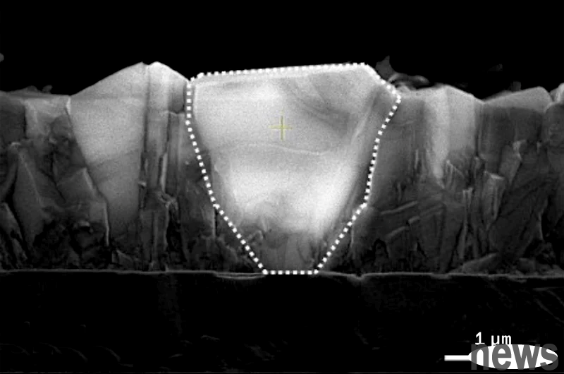
{twenty one} ▲ The boundary between diamond and semiconductor forms a thin layer of silicon carbide, which acts as a bridge for heat to flow into the diamond.In order to enable low-temperature growth, the team found a key chemical formula. Adding oxygen to the traditional methane and hydrogen mixture helps to continuously etch non-diamond carbon deposits. After extensive experiments, we found a formula that can grow large-grain polycrystalline diamond coatings below 400°C. This temperature is still within the tolerable range for CMOS circuits and other components.
Unexpected discovery of silicon carbide interface can overcome phonon bottleneckDespite the successful low-temperature growth of the diamond coating, the team still faces another challenge, which is Thermal Boundary Resistance (TBR), also known as the "phonon bottleneck." Phonons are thermal energy packets that accumulate at the boundaries of different materials, hindering heat flow, and reducing TBR has always been the goal of thermal interface engineering.
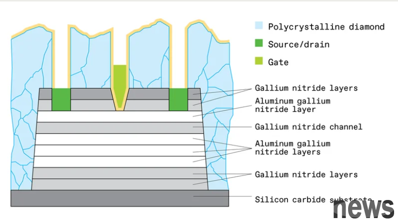 ▲ Gallium nitride high electron mobility transistors are an ideal test case for diamond cooling.
When the team grew diamonds on silicon nitride-covered gallium nitride (GaN), they unexpectedly observed that the measured TBR was much lower than expected. After collaborating with the University of Texas at Dallas on interface scientific research, it was confirmed that the formation of silicon carbide (SiC) is the cause of low TBR. The mixing at the interface between diamond and silicon nitride results in the production of silicon carbide, which can act as a phonon "bridge" to make heat conduction more efficient. The silicon carbide interface significantly improves the thermal performance of the component.
Early applications of gallium nitride and 3D CMOS wafers show potentialThe team first tested this low-TBR diamond coating on gallium nitride high electron mobility transistors (GaN HEMTs). GaN HEMTs are an ideal test case because the critical heat-generating part (the two-dimensional electron gas) is very close to the component surface. Early results are encouraging, with the addition of diamonds to GaN RF transistors reducing temperatures by more than 50°C. Lower temperature transistors amplify X-band radio signals five times better than before.
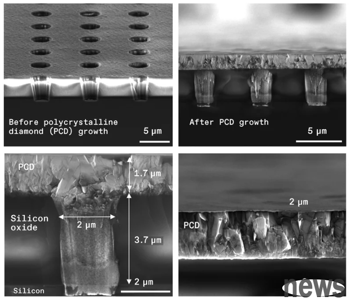 ▲ Polycrystalline diamond helps reduce the temperature of 3D chips. Diamond thermal vias are grown in micron-deep holes, allowing heat to flow vertically from one die to another die above the stack.
N-pole GaN HEMT, when the diamond layer completely surrounds the HEMT, the channel temperature drops by 70°C. This breakthrough could lead to transformational solutions for RF systems, allowing them to operate at higher powers than ever before. These results led the team to also set its sights on high-power CMOS wafers. For the 3D stacked wafer architecture, they proposed the concept of Thermal Scaffolding.
In the thermal skeleton concept, a polycrystalline diamond layer several nanometers thick would be integrated into a dielectric layer above the transistor to dissipate heat. These layers are then connected by vertical thermal conductors. These structures, called thermal pillars, conduct heat from one die to the next in the stack until the heat reaches the heat sink. After certification, in a dual-die stack structure, using diamond heat sinks and thermal pillar architecture, the temperature can be reduced to 1/10 of that without a thermal skeleton. Simulations show that in AI accelerators with more than five layers, the role of the thermal skeleton is critical, otherwise temperatures will far exceed typical limits.
Industrial collaboration and future prospectsThis research has aroused strong interest in the chip industry, including major manufacturers such as Applied Materials, Samsung and TSMC. It also expands collaboration among competitors in the semiconductor industry through the Stanford SystemX Alliance and Semiconductor Research Corp. The team is even working with the Threads program of the U.S. Defense Advanced Research Projects Agency (DARPA) to use device-level thermal management technology to develop efficient and reliable X-band power amplifiers with a power density 6 to 8 times higher than current devices.
There are still challenges to overcome, though, especially how to make the top of the diamond coating atomically flat. But the researchers and their partners are convinced that this study offers a disruptive new path to thermal management. In the future, diamond cooling technology will follow the same trajectory and become a key driving force in making a new generation of electronic products no longer limited by thermal energy. If this research is successful, it will ensure that high-performance computing can continue to develop and will no longer be constrained by thermal energy.